PCBGolf: shrinking a CAN-FD dev board
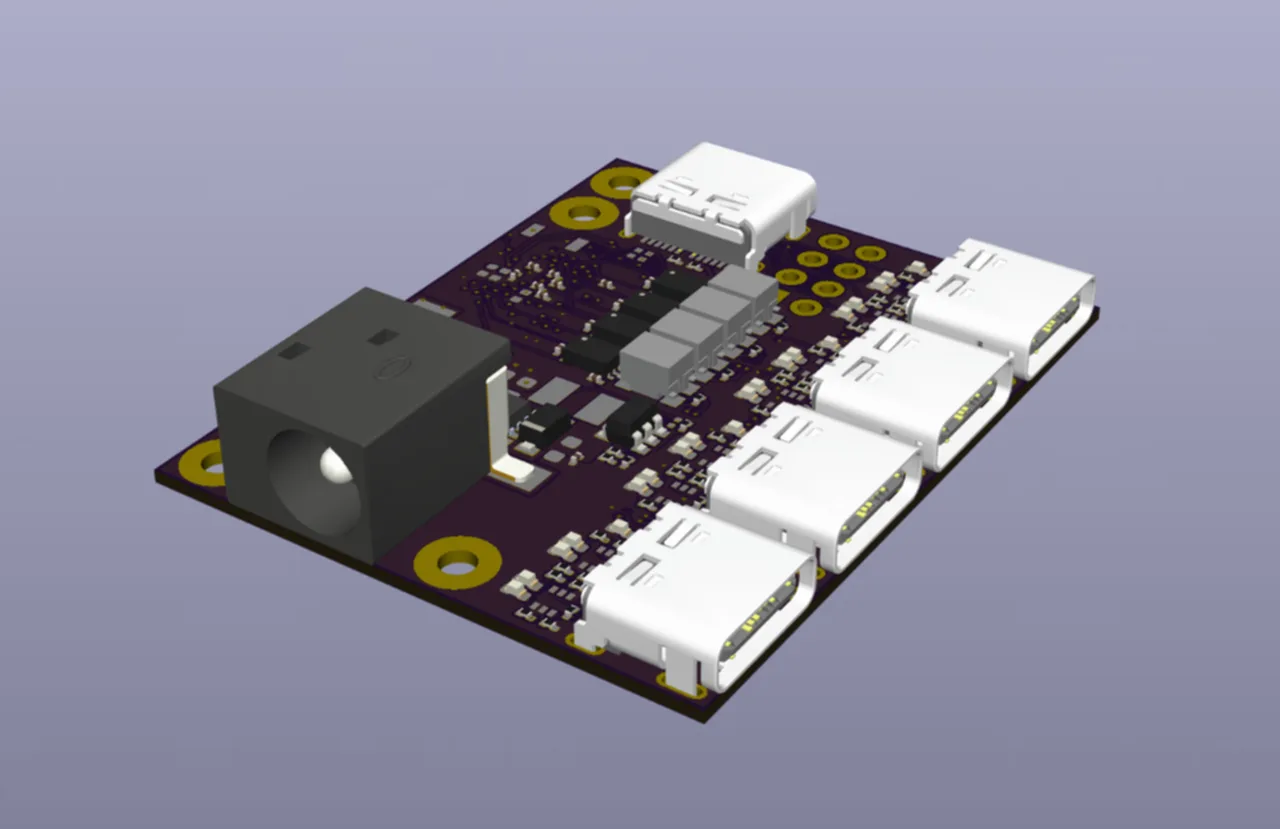
- Challenge
- comma.ai PCBGolf
- Layers
- 4, parts on both sides
- Outline
- 33.9 × 42.1 mm
- Height
- About 9.3 mm
- MCU
- STM32H725, TFBGA-100
- Score
- To come
comma.ai's PCBGolf challenge gives everyone the same board, loosely based on their panda jungle, and asks how small it can get. The board has a 12 V input with 5 V and 3.3 V supplies, four OBD-C ports with switched power and current monitoring, four CAN-FD transceivers, a USB hub, an STM32H725 and a microSD slot. Every interface has to keep working, mating connectors must stay compatible, and the board has to be manufacturable and assemblable at JLCPCB.
The score is the assembled board's bounding-box volume in mm³, plus 50 per via, plus 5000 per copper layer. Lowest wins.
Status: routing in progress. My score goes here once the entry is submitted.
What I changed
The schematic is comma's. I did the placement, the routing and the design decisions below.
- Stackup and placement. 4 layers: signal, power, ground, signal. Parts on both sides, with the STM32 and the USB hub on the bottom and the CAN parts and chokes on top.
- MCU package. The original is an LQFP-144. I first tried a UFBGA-169 at 0.5 mm pitch, which could not be escaped on 4 layers without blind or buried vias. The board now uses a TFBGA-100 at 0.8 mm pitch.
- Package change without touching the schematic. The BGA footprint's pads are renamed to the symbol's LQFP pin numbers, so the schematic still uses comma's symbol.
- Pins as a routing tool. Ports F and G do not exist on the smaller package, so 7 signals moved, including CAN2 to FDCAN3. I also re-ordered the 24 per-port control signals by channel to untangle the routing, keeping the current-monitor inputs on ADC pins. Both changes need matching firmware changes, which the rules allow.
- Smaller parts. 0201 and 0402 passives, smaller crystals, inductors, LEDs and FETs, and an SC-70 op-amp (TLV9101) in place of the SOT-23 one for the CAN LEDs.
- microSD. A stemless Molex 503398-1892 socket, 1.28 mm tall, on the bottom side.
- Power. The STM32 core runs from the chip's internal SMPS, set in firmware.
Design files
PCB layout (in progress)
Open in KiCanvasThe repo is at github.com/ulyssecrn/PCBGolf.
Lessons so far
- Layers and vias weigh more than size. One copper layer costs as much as 100 vias, so a 4-layer board starts 20,000 points behind before volume counts. A larger board on fewer layers can win.
- BGA pitch decides the layer count. The 0.5 mm package needed blind or buried vias to escape on 4 layers. The 0.8 mm one does not.
- One connector sets the height. The DC barrel jack accounts for about 75% of the board's total height.
- Pin assignment is a routing tool when the firmware follows it.